Based on those articles, an 807 STC amplifier of Kamijo's version 3 type was built for experimental purposes, and evaluated. The sound quality showed a distinct improvement over that of conventional circuits. Afterward several STC amplifiers of Kamijo's version 1 type, (plate to grid NFB based), were tried, as the circuit is simpler than that of the version 3 (plate to cathode NFB based).
Later prototype circuits built by the author have all been the version 1. Version 1 and version 3 are refered to as V1 and V3 in the following text. This article is based partially on Mr. Kamijo's V1. The differences between the V1 and V3 are detailed at Mr. Kamijo's own home page (at http://www.ne.jp/asahi/evo/amp/guide.htm).
Recently, Mr. Kamijo defined the new name "Voltage-Feedback-Tube" which is identical to auther defined name "Driving-Triode",
the auther updated related portion of this article on 1999/8/31 (Rev3.3).
However, experiments went further, until it was evident that any kind of power tube can be or should be applicable to the STC circuit. So, many kinds of power tubes were tried, either examples to hand or bought for the purpose of trialing. Now new trials have just started, using TV horizontal amplifier tubes and some kinds of transmitter tubes.
Data in this article is based on such tubes in the author's own stock;
some brand new, some others second hand. It also is to be noted that operating voltages and other parameters are not precisely those specified for the tubes used; tubes may not be operated at precisely optimum condition.
But allowing for slight deviations of individual tubes from specification, the author is confident that these tubes are operated with reasonable and safe margins.
The operation was checked by playing and listening to music and confirming that no odd or bad sounds were heard.
It is recommended that the constructor try variation of operating parameters when building and tuning an STC amplifier.
The adjustment procedure is described in "3.1 Adjustment of Bias Voltage".
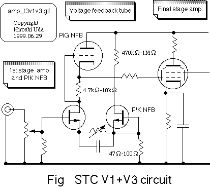
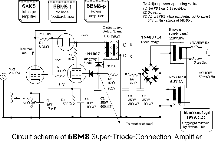
Figure 1; Schematic of a 6BM8 Super Triode Connection Amplifier
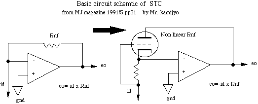
(1) A voltage-feedback-tube for high level plate to grid local NFB, controlled by a constant current source. Insertion of this non-linear element in the NFB is a very significant element of the topology.
(2) No overall NFB.
(3) Direct coupling.
(4) Insertion of a "Stopping Diode" and "Linearizer".
(A) First stage amplifier; the 6AK5 forms the voltage amplifier and constant current source.
(B) Driving-triode; the triode portion of the 6BM8 makes up the voltage converter, the driver for the final stage amplifier tube and constitutes the non-linear NFB element.
(C) Final stage amplifier; the pentode portion of the 6BM8.
(D) Stopping diodes; inserted in the B+ power supply side of the plate and/or screen grid circuit in the pentode portion of the 6BM8.
The second of the four features "No overall NFB." and the third item "Direct coupling" are already applied in conventional amplifiers.
The fourth item, the "Stopping Diode" and the "Linearizer" are new additions. The following subsections explain each of these four defining items in detail.
1.3.3.1 Even Semi-STC circuit, present effective STC sound.
The auther continued to try STC-rization of large amplitude requiring triode, such like UX2A3, applied P-G NFB'ed cathode follower drive circuit as follows.
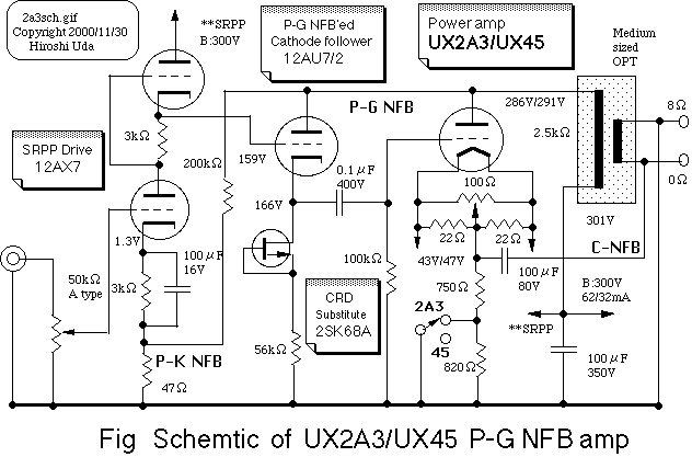
In above circuit, from the power supply voltage issue, hire a C/R coupling circuit. If a direct coupling circuit would be applied, about 150V or more of bulk voltage should be stacked up.
As for P-G NFB, (1) The internal impedance of cathode follower tube "Ri", will be round 10k ohms or more. (2) The current regulated diode (CRD) and resistor inserted to the cathode "Rk", will be round 100k ohms or more. So, by the relation of Ri < Rk, signal generated from the plate of final stage tube will be returned round 90 pecent to the grid of final stage tube. This situation makes final stage amp deep P-G NFB condition and voltage gain by "Mu" of final stage tube will be suppressed to nearly 1. However, the current component generated by the mutual conductance "Gm" is kept untouched.
1.3.3.2 STC circuit may be configured by driver stage and final stage
Thus, the deep P-G NFB conditioned final stage amp is a prototype of STC version 1 amplifier. However, enough amplitude of input signal should be supplied to the grid-ground of the cathode follower tube.
In case large amplitude requiring triode, SRPP pre-driver with high Mu voltage amplifying triode would be required. In case tetrode/pentode,
simple high Mu voltage amplifying triode would be enough to drive.
1.3.3.3 STC V1 circuit
The circuit STC V1, insures the voltage gain by signal input between the grid-cathode of cathode follower tube. Then the "voltage feedback tube" acts not only for the NFB, but also acts as a voltage amplifier also. Load of amplifier is the CRD and resistor inserted to the cathode, that is the first stage amplifier by voltage amplifying pentode or FET/bipolar-transistor. The naming "voltage feedback and amplifying tube" of that tube would be more suitable.
And also in the STC V1 circuit, signal input to final stage is done from cathode of voltage feedback tube. This connection eliminates the effect of grid current from final tube and makes stable the whole circuit.
(2001/4 Rev3.11)
The basic circuit of the STC consists of the following three functional elements.
Name of tubes and releavant circuits
Formerly, the naming of the driver stage was not specifically determined in Mr. Kamijo's article; the auther defined the simple name as "Driving-Triode".
Afterwards, Mr. Kamijo defined the name as "Voltage-Feedback-Tube", the auther update this article according to the new deffinition.
To the first stage amplifier, which acts as a V/I convertor and constant current source, the auther gave the simple name "1st stage".
As for the final stage amplifier; "final stage (amplifier)".
Through this paragraph, some readers may feel some difficulty understanding the operation fully.
So the most critical points are clarified through the following explanation. In order to understand the following section, it is necessary to know the "Three constants of the vaccum tube".
Consider how the "Mu"= 1 operation described later is realized, and how the constant current source works.
Constant current source
In a circuit which has a constant current source (here-in-after called CCS) character, when a
given voltage is varied, the current does not vary (much). For example,
a component called a "Constand current diode" has such a character. And
also pentodes, bipolar-transistors, and FET's have the same character.
The reason to utilize the constant current source, will be explained later.
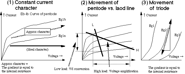
Refer to the figure "Figure 3 Character of a Constant Current Source etc.".
Constant current source by pentode
Refer Figure 3(1), The figure explaines how the Character of a CCS can be obtained from the Eb-Ib characteristic of a pentode, with its high internal resistance character.
V/I conversion by pentode
Refer Figure 3(2), The figure explaines how the function of V/I conversion can be obtained from the Eb-Ib characteristic of a pentode with smaller load.
Voltage amplification by pentode
Refer Figure 3(2), The figure explaines how the function of amplification can be 0btained from the Eb-Ib characteristic of a pentode with larger load.
Co-existence of CCS function and V/I conversion of function by pentode
Refer Figure 3(2), The figure explaines the co-existence ob both CCS
and V/I conversion of a pentode with smaller load.
Characteristic of triode
Refer Figure 3(3), The figure explaines the low internal resistance character of triode.
Now, return to the main subject;
Mr. Kamijo further explains;
"(1) The amplification factor of the final stage will be unity, where 100% NFB is applied". This expression means that if the final stage has full amplitude NFB applied, then the final stage tube doesn't work as a voltage amplifier, just as a V/I converter (Figure 4.1/4.2). The current conversion performance is simply determined by the mutual conductance, gm, of the output pentode. Also in his article, Mr. Kamijo says;
"(2) The total gain of the voltage-feedback-tube (here-in-after called VFT) and the final tube combination is approximately equal to the amplification factor, "Mu", (which is written with the same Greek symbol as "Micro"), of the VFT".
Tracing the circuit, the following points become clear.
In the normal amplification circuit, the sequence of element will be arranged as ground - amplification element - load - power supply - and return to the ground.
In above two circiuits, the sequence is invereted as
ground - load - amplification element - power supply - and return to the ground. However the operation of amplification suffers no effect by this
inversion. Actually such inversion can be oftenly seen in the SEPP/OTL circuits.
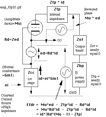
The output transformer (here-in-after called OPT) and the B+ power supply are in the signal loop. However the impedances of these intervening elements are far smaller than that of the constant current source. The function of the CCS is to keep the degree of plate to grid NFB at maximum.
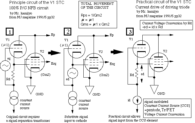
1st stage tube convert input voltage signal "ei" to current signal "id" with its mutual conductance "Gm1";
id = ei*Gm1 (where * means mltiplication operator )
The resistance located in the cathode of VFT called "Rd" convert "id" to "ed" by the multiplication;
ed = Rd*id
After this I/V conversion being done, further circuit operation is identical to the Theoretical circuit/ Cathode input descrobed on paragraph 1.4.2.2.
However, in above described operation, some undesired effect will be occured in the VFT. That is the incurrence of reversed phase signal generated from internal impedance of VFT(Ztp) with "id" I/V conversion;
Ztp*id.
Precisely the total amplitude of VFT should be expressed as;
Mu*ed - Ztp*id = Mu*Rd*id - Ztp*id
The signal, amplified by the VFT, appears as (Mu-1) in amplitude, between the grid and cathode of the final stage.
The meaning of the -1 term is as follows.
The signal is fed from the cathode of the VFT, and the source signal to the VFT is that between the cathode of the VFT and ground; i.e. the CCS; this signal is reversed in phase with respect to the amplified signal.
However, in practice, the mu value of a typical triode will be greater than 10, and so the effect of the -1 term will typically be negligible.
Finally, the driving voltage for the final stage "Efdr" is;
Efdr = μ*Rd*id - Ztp*id - Rd*id = id *{Rd*(μ-1) - Ztp}
Refer Figure 4.3 Operation of Practical Circuit.
The principle "Mu"= 1 means current conversion operation
The basic operational circuit may be broken down, on a signal handling
basis, to help explain the operation, as follows;
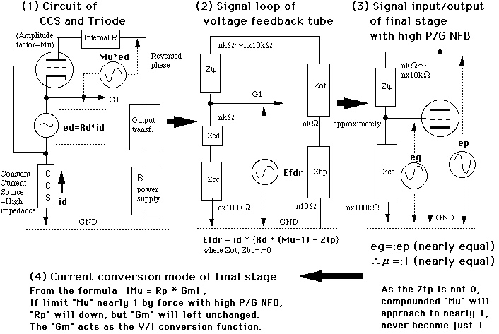
Fig 5(1) shows the amplification operation of the VFT.
The signal "ed" input to the cathode, is amplified, and the output
signal appears as "Mu*ed" in amplitude, reversed in phase.
Fig 5(2) shows the elements, and their approximate impedance values,
that are involved in the amplification of the VFT.
Zcc: Impedance of the constant current source
Zed: Impedance of the signal source
Ztp: Impedance of the triode i.e. internal resistance
Zot: Impedance of the output transformer
Zbp: Impedance of the B power supply
Fig 5(3) shows nearly 100% NFB, that is a "Mu"= 1 operational mode.
Strcitly speaking, the triode has five load impedances to be considered.
However the dominating impedance will be Zcc.
Then the signal appearing between Zcc and ground, is input to the final stage. The operation of the final stage is as follows.
The amplified signal voltage appearing on the plate, will returned
to its grid.
Zcc/(Ztp+Zcc)....Nearly equal to 1, whereas Zcc is far greater than Ztp.
This operation means nearly 100% voltage NFB, and it also means no voltage amplification being done by the final stage.
Fig 5(4) shows the principle of the current conversion function. Then the circuit might be calleded a {Current conversion amplifier} or a {Gm amplifier}, and these would be more suitable than "STC".
(C) The need for the constant current source (CCS)
At first glance, the reader will ask "Why do they use the CCS? Can't
the CCS be simply replaced by a capacitor or resister?" Using a CCS is
most important. The operation of the CCS is as follows. In the low voltage
area (see Figure 3), current climbs with a steep slope, but after the
early rise, the slope changes to a more gradual one.
This character of the CCS is very convenient for realizing a constant current character with a low supply voltage. To realize such a circuit characteristic with just a high valued resister, and to make a similar gradual V-I slope, would require a high value minus power supply, to pull down the other end of the resister. So the CCS is an essential element to facilitate voltage distribution and signal handling functions together, in the STC-V1 direct-coupled circuit environment.
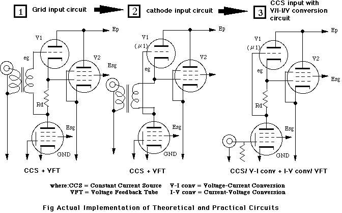
(1) The input signal controls the CCS, which is the first stage.
(2) The plate current is "modulated" by the input signal as "id".
(3) The resistor inserted in the cathode of the VFT converts the signal-modulated current to a voltage,
(4) The VFT amplifies the voltage signal using a grounded grid amplifier.
At first glance, this circuit looks like an SRPP. However, using plate to grid NFB (P-G NFB) as well, changes the operation of the VFT to the following combination of functions;
(1) An amplifier performing current to voltage conversion of the input signal.
(2) Non-linear element inserted in the plate to grid NFB (P-G NFB).
(3) Cathode follower driver for the final stage, providing low impedance drive and protect malfunction of CCS when final stage tube begin to flow grid current with over swing.
The actual element of the 1st stage tube, which has the constant current source function as well, can be a voltage-amplifier pentode, a BJT, or a FET [where BJT Bipolar Junction Transistor, FET = Field Effect Transistor]. This element voltage-amplifies the input signal and converts it to current amplitude. So, from the viewpoint of circuit operation, the first stage amplifier and the circuit of VFT of the V1 STC circuit obviously differ from a conventional SRPP circuit.
The effect of the SD is not merely specific to the STC amplifier however. It is also effective in other non-NFB or local NFB amplifiers. In the case of overall loop NFB amplifiers, the effect does not appear at all or is reduced. Supposedly, the reason is that overall loop NFB amplifier acts to amend the shape of signal waveforms passing through, by NFB action.
In an ideal amplifier, the final stage tube acts as a signal source and the output transformer acts as a load. The power supply should ideally have zero internal impedance. These three circuit elements constitute a DC loop, although the power supply itself is not involved with the signal path, as such.
Just the signal source and the load on the DC loop should share the signal power. The DC loop is essential however, to convey the signal power. There will be some impedance mismatching between the signal source and the load. The mismatch means that power is partially "pushed" through the output transformer, with a remaining portion absorbed and dissipated by the signal source, i.e. the final stage tube.
Further, the B+ power supply should contain enough energy storage capacity to support the amplifier's transient power requirements. It should contain about 5 or more times the "micro F" of capacitance as the nominal B+ current in "mA". For example, an amplifier that requires about 200mA DC at no-signal, should preferably have a capacity of (5 x 200 ) 1,000micro F or more. This requirement for large capacitance yields a power supply with less internal DC resistance; that is to say, one providing close to the performance of an ideal power supply.
The operation of a Linearizer is by virtue of a serially connected amplifier element and compensating element. The former element amplifies the input signal and its output includes non-linear distortion. Then the latter (linearizing) element reforms and/or absorbs the distortion by applying the reverse of the original non-linear characteristic. For example, such circuits as the differential amplifier and/or SRPP look like having latent lineariser functions.
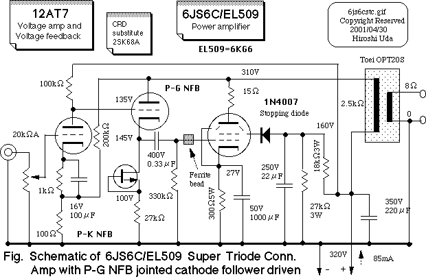
(1) In the MJ Magazine 1992/10, Mr. Kamijo described an EL86/6CW5 STC SRPP amplifier.
(2) An associate of the author has tried an STC driven, non-NFB, SE amplifier. The author also tried this, in a CV18 direct coupled grounded grid amplifier.
(3) The same associate also tried an STC push-pull amplifier, but it didn't sound so good.
Anyway, in listening tests the impression of the audience is typically
"Clear and powerful sound", "Delightful sound", and "There is no resistance
to making the volume larger" and so on.
As for the overall effectiveness of the STC circuit, it appears (beam)
tetrode and pentode power tubes give a very good result, while triode power
tubes are somewhat poor.
(1) Combination of pentode voltage amplifier and CCS, and VFT
or
(2) Combination of BJT/FET voltage amplifier and CCS, and VFT
The first issue to be noted, to impliment these topologies, is as follows. With a pentode for the 1st stage amplifier, the supply DC voltage for the screen grid should be precisely set. If this voltage is too low, correct operation of the 1st stage amplifier, and consequently the whole amplifier, is not assured. For example, while the 6AK5/6AS6 requires only a low voltage - around 30V, correct operation for a 6AU6 requires a minimum of 45V, and so on.
The value of the resistor for the cathode of the final power stage should then be calculated as follows. The cathode voltage (typically approximately 50V~70V) equals the sum of the normal self bias (V) for the final tube, plus "bulk" voltage for the screen grid of the 1st stage tube. The circuit will work even if at higher or lower than this calculated value. However to ensure sufficient signal amplitude from the 1st stage amplifier, the voltage should err on the high side to some extent. Additional voltage is further required to ensure correct operation of the VFT.
Consideration is now given to the "balance" or distribution of the operating voltages for both the 1st stage and the VFT.
In the case of a tetrode or pentode final stage, no trouble occurs as long as sufficient supply voltage is available. In case of a triode final stage, the bias voltage is higher than that for the tetrode or pentode topology, so some manipulation of the distribution of the supply voltage or the "bulk" voltage is required.
In most cases, after construction is finished, testing can be started immediately. Check the cathode voltage of the final tube and adjust the cathode bias voltage of the 1st stage amplifier, using VR, to set the grid voltage of the final stage tube. Detailed adjustment procedures are described in the later section "3.1 Adjustment of the Bias Voltage of the Final Stage".
FB tube |
(mA) |
|||||||
| 6AN5 | 2SK68A | 5965/2 | 120/120 | -6.7 | 40 | 34 | 1200 | |
| 6AQ5 | 2SK68A | 12AX7/2 | 240/200 | -12.5 | 60 | 30 | 1560 | 6DS5 amp |
| 6AR5 | 2SK68A | 12AX7/2 | 235/195 | -18 | 65 | 33 | 1560 | 6DS5 amp |
| 6AS5 | 2SK68A | 12AT7/2 | 110/110 | -8.5 | 40 | 40 | 1000 | |
| 6AU5GT | 6U8A-p | 12AX7/2 | 220/150 | -20.0? | 60 | 45 | 1320 | |
| 6AV5GA | 6U8A-p | 12AX7/2 | 220/145 | -22.5 | 50 | 61 | 820 | |
| 6AW8A-p | 6AS6 | 12AT7/2 | 210/165 | 180Ω | 55 | 14 | 3660 | |
| 6BK5 | 6AK5 | 12AT7/2 | 290/280 | -5 | 58 | 38 | 1500 | |
| 6BM8-p No.1 | 6AK5 | 6BM8-t | 210/210 | -16 | 44 | 37 | 1200 | |
| 6BM8-p No.2 | 2SC1775A | 6BM8-t | 220/190 | -16 | 42 | 34 | 1200+47** | 47Ω for Tr |
| 6BQ5 | 6GH8A-p | 6GH8A-t | 260/230 | -7.3 | 50 | 42 | 1200 | |
| 6CL6/6197 | 6AS6 | 12AT7/2 | 200/150 | -2 | 44 | 37 | 1200 | →6AG7 |
| 6CW5 | 6BX6 | 12AX7/2 | 140/140 | -12.5 | 60 | 68 | 880 | |
| 6DQ6A/B | 6U8A-p | 12AX7/2 | 240/140 | -22.5 | 51 | 62 | 820 | |
| 6DS5 | 2SK68A | 12AX7/2 | 250/210 | -8.5 | 50 | 32 | 1560 | |
| 6F6G/GT/42 | 6GH8A-p | 12AX7/2 | 250/210 | -16.5 | 60 | 38 | 390+1200* | 46V→SG |
| 6G-B7 | 6BL8-p | 12AT7/2 | 215/120 | -22.5 | 55 | 50 | 1100 | |
| 6GW8-p | 6AK5 | 6GW8-t | 245/230 | -7 | 50 | 42 | 1200 | =ECL86 |
| 6HZ8-p | 6AS6 | 12AT7/2 | 200/150 | 100Ω | 52 | 30 | 1680 | |
| 6K6GT/41 | 6GH8A-p | 12AX7/2 | 250/170 | -18 | 60 | 38 | 390+1200* | 46V→SG |
| 6L6GB/GC | 6BL8-p | 6BL8-t | 290/270 | -14 | 60 | 73 | 820 | |
| 6LR8-p | 6BL8-p | 6LR8-t | 210/110 | -10 | 60 | 60 | 1000 | |
| 6R-HP3-p | 6AK5 | 6R-HP3-t | 175/125 | ? | 60 | 32 | 2000 |
FB tube |
(mA) |
|||||||
| 6V6G/GT No.1 | 6EA8-p | 6EA8-t | 250/250 | -12.5 | 56 | 47 | 1200 | |
| 6V6G/GT No.2 | 6GH8A-p | 12AX7/2 | 250/210 | -12.5 | 60 | 38 | 390+1200* | 46V→SG |
| 6Y6G/GT | 6BX6 | 6SL7GT/2 | 190/135 | -14 | 60 | 60 | 1000 | |
| 12A6 | 6U8A-p | 12AT7/2 | 225/230 | -12.5 | 74 | 30 | 680+1800* | 54V→SG |
| 12BY7A | 6U8A-p | 12AX7/2 | 240/190 | -2.6 | 46 | 29 | 1600 | |
| 30A5 | 2SK30A-Y | 12AU7/2 | 100/100 | -4.7 | 38 | 38 | 1000 | |
| 38 | 6U8A-p | 12AT7/2 | 245/250 | -25 | 65 | 26 | 680+1800* | 48V→SG |
| 807/1625 | 6BL8- | 12AT7/2 | 250/245 | -14.5 | 65 | 80 | 820 | |
| 1619 | 6U8A-p | 12AX7/2 | 280/240 | -10 | 50 | 42 | 1200 | |
| 6146 | 6U8A-p | 12AX7/2 | 290/170 | ? | 60 | 52 | 1160 | =S2001/A/M |
| 6360 para | 6U8A-p | 12AT7/2 | 190/140 | -7.5 | 55 | 67 | 820 | parallel use |
| 6384 | 6U8A-p | 12AT7/2 | 235/215 | -22.5 | 65 | 74 | 880 | =6AR6 |
| 6550C/KT88 | 6U8A-p | 12AX7/2 | 290/270 | -14 | 65 | 79 | 820 | |
| CV450 | 6U8A-p | 12AX7/2 | 240/140 | -22.5 | 50 | 61 | 820 | =6CU6 |
| EL33 | 6EA8-p | 6EA8-t | 250/250 | -4 | 50 | 42 | 1200 | |
| EL34/6CA7 | 6BL8-p | 6BL8-t | 290/270 | -14 | 60 | 73 | 820 | |
| EL509 | 6U8A-p | 12AX7/2 | 315/185 | ? | 75 | 91 | 820 | =6KG6 |
| WE350B | 2SK30A-Y | 6N7GT | 215/180 | ? | 35 | 70 | 500 | Mr. Yamada |
(a) 6AC5GT "Mu" 58; an exceptionally high "Mu" value. It is driven by a direct coupled UY56/UY76 or 6P5GT.
(b) 6BX7GT "Mu" 10; a typical modern triode.
(c) 6EM7 "Mu" 5.4; a typical TV horizontal driver.
(d) 6AS7G "Mu" 2; an exceptionally low "Mu" voltage regulator tube.
Generally, high "Mu" triodes require low grid bias voltage, and have high internal impedance.
A low "Mu" triode requires a high bias voltage, and has low internal impedance. Exceptionally, some kinds of triode, such as the 6AC5GT, require positive grid bias voltage drive and current mode drive.
In another exceptional instance, some kinds of transmitter tube, such as the 811 and CV18, have two characteristic operational domains. In the minus bias domain, they work as a normal triode, and in the positive bias domain they work with lots of grid current.These kinds of triode require low impedance driving techniques to yield full power operation.
Generally speaking, some countermeasures to allow for variations in individual tube characteristics will be required to operate a triode output tube properly in an STC amplifier. The areas of concern include the following.
(a) Large drive amplitudes are required.
(b) There is a tendency to lack sufficient drive voltage output from the 1st stage amplifier, when the circuit is configured with a pentode and VFT combination.
(c) There is difficulty adopting a direct coupled final stage topology, and operation with its high bias voltage, from a single B+ power supply.
The characteristics of a power triode tube require a multi voltage power supply, or a fixed minus bias power supply for the first stage amplifier, and/or input signal separation with an input transformer, etc. at the same time.
To implement a power triode amplifier, the required amplitude of driving voltage can be roughly estimated by calculation from the bias voltage. The required driving voltage
Vd (peak to peak) bias voltage x square root of 2.
Consider for example, the 2A3 triode, which requires 45V bias voltage. Vd would be around 63V.
It is easily imagined that such a value cannot be realized by a combination of voltage amplifier pentode and VFT or the combination of BJT/FET and VFT. In these cases, to drive the power triode fully, the following countermeasures are required.
(1) A high voltage power supply is required for the pentode and VFT combination.
(1.1) An additional power supply cascaded on the main power supply may be needed for the final stage.
(1.2) Alternately, the cathode and G1 of the voltage amplifier pentode could be taken to a negative power supply. In this case, a signal separation transformer should be inserted into the input signal line.
(2) Utilizing a conventional SRPP, to get enough drive signal amplitude.
The above points notwithstanding, listening tests with a 6EW7 V1 STC amplifier in under-powered condition, showed that enough volume was available, even in an incompletely driven amplifier.
In case a power troiode with pentode and VFT configuration applied, the screen grid voltage for first stage amp. fed from the cathode of final tube, should be "round bulk voltage" i.e. lower than corresponding bias voltage of the power triode as shown in the "Table 2; Example of Operation of a STC V1 SE Amplifier" in section 2.4.4 Example of Triode Operation.
This voltage distribution makes triode-STC operation stable. (2000/5/8)
With this circuit, the NFB section conforms to the V1 STC circuit. However the constant current source function of the 1st stage amplifier may not qualify. The reason is that the 1st stage amplifier is a rather pure voltage amplifier and has no constant current characteristics. Through experiment with this NFB'ed SRPP circuit, which, like an incomplete STC circuit, looks like having plate to grid NFB applied to some extent, the sound obtained appears a little similar to the sound of a standard STC V1 circuit.
Obviously there will be an accuracy difference in the operation of the circuit, between a pure SRPP directly connected to the B+ power supply and the SRPP used together with plate to grid NFB. It is assumed that the latter circuit would have some current mode driving function to the final stage. This circuit is refered to in this text as the "SRPP drive" to distinguish it from the pure STC, as the operation of the two differs.
| 1 | 1.0 | 2 | 62 | 12 | 2.3 |
| 2 | 0.5 | 4 | 90 | 10 | 2.0 |
| 3 | 0.0 | 10 | 165 | 7 | 1.4 |
| 4 | -0.5 | 15 | 235 | 4 | 0.8 |
| 5 | -1.0 | 20 | 295 | 1 | 0.2 |
FB tube |
(V/mA) |
|||||||
| 6BQ5(T) | -10 | 19 | 6U8A-p | 12AX7/2 | 220/38 | 46 | 1200 | |
| 76-6AC5GT** | -13.5=76 | 58# | 6U8A-p | 12AX7/2 | 250/36 | 54 | 1500 | #μ=6AC5GT's |
| 6G-A4 | -19 | 10 | 6U8A-p | 12AX7/2 | 250/40/TD> | 62 | 390+1200* | 46V→SG |
| 6R-A8 | -19 | 9.7 | 6U8A-p | 12AX7/2 | 235/41 | 65 | 390+1200* | 46V→SG |
| 12B4A | -22 | 6.5 | 6AS6 | 12AT7/2 | 200/22 | 65 | 620+2700* | 47V→SG |
| 6AH4GT | -23 | 8 | 6U8A-p | 12AX7/2 | 250/24 | 60 | 820+1640* | 40V→SG |
| EL34(T) | -26 | 11 | 6U8A-p | 12AX7/2 | 250/50 | 60 | 390+820* | 40V→SG |
| 6EW7*** | -40 | 6 | 6U8A-p | 12AX7/2 | 200/36 | 80 | 1000+1200* | 45V→SG |
It is possible to configure the whole STC amplifier by using just "one" B+ power supply. The adjusting process of the bias of the final stage tube is explained for this set-up. The following steps are required to set up an STC amplifer for proper operation.
(1) Set the bias of the first stage voltage amplifier, pentode or BJT/FET, to a low level initially, using VR2 (variable resistor). In this condition, the first stage amplifier is set to a low internal resistance state. Then the greater portion of the voltage output from the plate of the final stage tube will be carried by the VFT.
(2) In this condition, the grid of the final stage tube is at lower than normal bias voltage. Also the voltage on the screen grid of the first stage amplifier is lower than normal, and operation of the STC will be incorrect and it'll have heavy distortion.
(3) Now slowly increase the resistance of the VR2 in the cathode (emitter/source) of the 1st stage amplifier. The operation of the STC will gradually become normal. In this condition, measure the cathode voltage of the final stage tube. Calculate the cathode current using the fomula;
cathode current (Ik mA) = cathode voltage (Vk Volt) / cathode resistance (Rk Ohms)
Ensure that the operation of the final stage tube is within the tube's data sheet specification limitations.
(4) Then find the most powerful or most favourable operating point of the final tube, within its specification limits.
(5) If the adjustment failed, check and vary the cathode resistors of the VFT and the final stage tube. Find a proper operational point, by repeating steps (1)~(4) above.
In a very few cases this step (5) adjustment was required in the author's early experimental stages. In such cases, the voltage of the cathode of the final stage tube was insufficient. If a BJT/FET is employed as the 1st stage amplifier, this adjustment will be somewhat critical.
Essentially the operation point of the first stage and the operation point of the final stage should be independent. However, the STC V1 circuit is adjusted by only one variable resistor in the 1st stage, for convenience. So a circuit adjusted for the best point of the final stage doesn't mean the setting of the 1st stage is at the best point.
If the 1st stage can tolerate a wide latitude of operating voltages, then the 1st stage can produce proper operation even though its setup voltages are not precisely suitable.
In most examples of the author's designs, using newly tested tubes, the cathode current of the final stage was initially determined and then the cathode voltage, giving the required value of cathode resistance. After doing this design step, the voltage will, in practice, be within plus or minus 10% of this calculated value. The voltage supplied to the 1st stage may be varied from the best point, as its operation is not as critical as that of the final stage.
In most cases, the STC V1 amplifier can be adjusted to approximately the correct operating point. In a few worst cases, the author had to change and adjust the cathode resistance of the final stage, to give correct operation of the 1st stage.
In the case of FET's the author experienced troubles to some extent. Varying the drain operating voltage had some subtle impact on the sound. Depending on the actual type of FET used, the sound quality varies, depending on the drain voltage it's operated at. The latitude of favourable sonics is generally narrow with some kinds and wide with others. In the worst case the cathode resistance was changed to get the optimum "bulk" voltage for the FET.
From this viewpoint, the pentode is most favourable with regard to set-up and adjustment.
However, the clipping will begin from the cut-off side of the final tube. Never set the operational point to exceed the maximum plate passivation power limit, even if the clipping balance is in asymetric. (2000/7/22)
The way to get a lower voltage is very simple. By dividing the cathode bias resistor of the final stage, an adequate screen grid voltage will be obtained. Then it is possible to realize both high bias levels for the final stage and proper screen grid voltage at the same time.
In Table 1; Example of Operation of an STC V1 SE Amplifier using a Tetrode or Pentode Output Tube and Table2; Example of Operation of an STC V1 SE Triode Amplifier, the divided cathode resistor for the screen grid is applied in several examples.
6AS6 - 12AT; up to around 250V
6U8/6BL8 - 12AT7; ditto
6AK5 - 6AT6 (triode of 6BM8); ditto
6AU6 - any voltage amplifier triode; ditto, but the voltage for the
screen grid should be over 45V
Any kind of voltage amplifier pentode - 12AX7; 250V or more
The supply of the 1st tube's screen voltage by the cathode bias of the final tube makes the issue somewhat complicated. However the parts count is reduced by this method. A systematic investigation is required of this area in the future.